Sharan Nagesh's Email & Phone Number
Graphics Hardware Engineer at Intel Corporation
Sharan Nagesh Email Addresses
Sharan Nagesh's Work Experience


Intel Corporation
Graphics Hardware Engineer
January 2016 to January 2019
Intel Corporation
PDG- Peripheral Connectivity Hub Circuit Design Engineer Intern
January 2015 to January 2015
Show more
Show less
Sharan Nagesh's Education
The University of Texas at Dallas
January 2013 to January 2015
Bangalore Institute Of Technology
January 2009 to January 2013
Show more
Show less
Frequently Asked Questions about Sharan Nagesh
What is Sharan Nagesh email address?
Email Sharan Nagesh at [email protected] and [email protected]. This email is the most updated Sharan Nagesh's email found in 2024.
How to contact Sharan Nagesh?
To contact Sharan Nagesh send an email to [email protected] or [email protected].
What company does Sharan Nagesh work for?
Sharan Nagesh works for Intel Corporation
What is Sharan Nagesh's role at Intel Corporation?
Sharan Nagesh is PDG- Peripheral Connectivity Hub Circuit Design Engineer Intern
What is Sharan Nagesh's Phone Number?
Sharan Nagesh's phone (213) ***-*236
What industry does Sharan Nagesh work in?
Sharan Nagesh works in the Semiconductors industry.
Sharan Nagesh's Professional Skills Radar Chart
Based on our findings, Sharan Nagesh is ...
What's on Sharan Nagesh's mind?
Based on our findings, Sharan Nagesh is ...
Sharan Nagesh's Estimated Salary Range
Sharan Nagesh Email Addresses
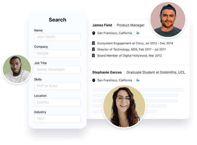
Find emails and phone numbers for 300M professionals.
Search by name, job titles, seniority, skills, location, company name, industry, company size, revenue, and other 20+ data points to reach the right people you need. Get triple-verified contact details in one-click.In a nutshell
Sharan Nagesh's Ranking
Ranked #1,013 out of 20,260 for PDG- Peripheral Connectivity Hub Circuit Design Engineer Intern in California
Sharan Nagesh's Personality Type
Introversion (I), Intuition (N), Thinking (T), Judging (J)
Average Tenure
2 year(s), 0 month(s)
Sharan Nagesh's Willingness to Change Jobs
Unlikely
Likely
Open to opportunity?
There's 100% chance that Sharan Nagesh is seeking for new opportunities
Top Searched People
Former First Lady of the United States
American actress
Singer and actress
YouTuber
Aruban baseball shortstop
People you may be
interested in

Owner at Barron's Outfitters

Vice President of Customer Experience Strategy at Infineon Technologies

R&D Manager at TSMC North America

Senior Director Of Engineering at Samsung Semiconductor
Senior Director of Sales at UTAC

Account Director - US East at GLOBALFOUNDRIES

Owner at Paul Clowes Consulting Ltd.
Director Of Corporate Partnerships at MDR Education Marketing Services and Solutions
Asst Track Coach - Sprints at Trabuco Hills High School

Supply Chain Analyst at Boeing

Venice Beach to Mars at Delancey Street Press
Adjunct Faculty at Riverland Community College


Sharan Nagesh's Social Media Links
/in/sharannagesh