Vivek Surabhi's Email & Phone Number
Staff Design Engineer (Autonomous Driving Platform)
Vivek Surabhi Email Addresses
Vivek Surabhi's Work Experience


Innovusion Inc
Senior FPGA Design Engineer
April 2024 to April 2024


Genesis Microchip
Intern
April 2024 to April 2024
Villanova University School of Engineering
Graduate Teaching Assistant
April 2024 to April 2024
Villanova University School of Engineering
Lab Administrator Trainee
April 2024 to April 2024

Show more
Show less
Vivek Surabhi's Education
Visvesvaraya Technological University
Bachelor of Engineering, Electronics and Communication
April 2024 to April 2024
Villanova University
MS, Computer Engineering
April 2024 to April 2024
Show more
Show less
Frequently Asked Questions about Vivek Surabhi
What company does Vivek Surabhi work for?
Vivek Surabhi works for BYTON
What is Vivek Surabhi's role at BYTON?
Vivek Surabhi is Staff FPGA Design Engineer
What is Vivek Surabhi's personal email address?
Vivek Surabhi's personal email address is s****[email protected]
What is Vivek Surabhi's business email address?
Vivek Surabhi's business email address is vivek.surabhi@***.***
What is Vivek Surabhi's Phone Number?
Vivek Surabhi's phone (213) ***-*400
What industry does Vivek Surabhi work in?
Vivek Surabhi works in the Semiconductors industry.
Vivek Surabhi's Professional Skills Radar Chart
Based on our findings, Vivek Surabhi is ...
What's on Vivek Surabhi's mind?
Based on our findings, Vivek Surabhi is ...
Vivek Surabhi's Estimated Salary Range
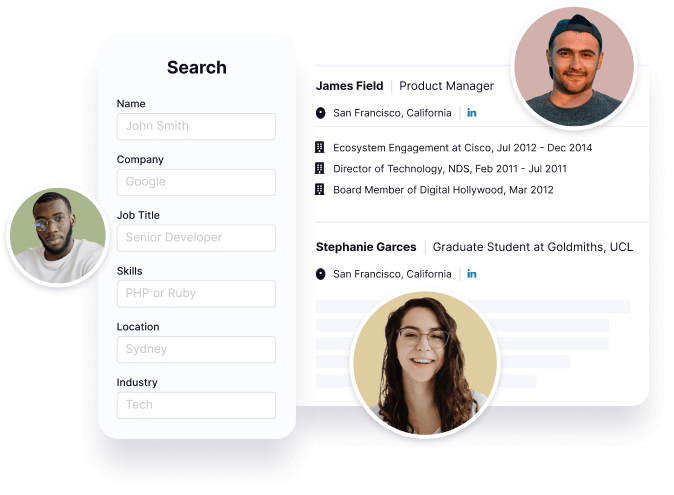
Vivek Surabhi Email Addresses
Find emails and phone numbers for 300M professionals.
Search by name, job titles, seniority, skills, location, company name, industry, company size, revenue, and other 20+ data points to reach the right people you need. Get triple-verified contact details in one-click.In a nutshell
Vivek Surabhi's Ranking
Ranked #1,393 out of 27,860 for Staff FPGA Design Engineer in California
Vivek Surabhi's Personality Type
Introversion (I), Intuition (N), Thinking (T), Judging (J)
Average Tenure
2 year(s), 0 month(s)
Vivek Surabhi's Willingness to Change Jobs
Unlikely
Likely
Open to opportunity?
There's 94% chance that Vivek Surabhi is seeking for new opportunities
People you may be
interested in

Product Manager at NVIDIA at ANSYS Apache
Sr. ASIC Design Engineer at NVIDIA at NVIDIA
GHC20 | Actively Seeking Full Time/Co-op Positions | MS in Software Engineering at San Jose State University at San Jose State University
Senior User Experience Designer at VMware at VMware
Staff Electrical Engineer at Verb Surgical Inc. at Verb Surgical Inc.
Staff FPGA Engineer at Vave Health at Vave Health
Staff FPGA Design Engineer at Zoox at Zoox
Design Engineer at Microsoft at Microsoft
Senior Staff Design Engineer at Black Sesame Technologies Inc at Black Sesame Technologies Inc
Staff Design Engineer at Intersil Corporation at Intersil (acquired by Renesas)
R&D Engineer at Broadcom Inc.
Senior Design Engineer at Optalysys at Coherix


Vivek Surabhi's Social Media Links
/in/vivek-surabhi-137b0342 /school/villanova-university/ /company/verb-surgical