Scott Williams's Email & Phone Number
American basketball player
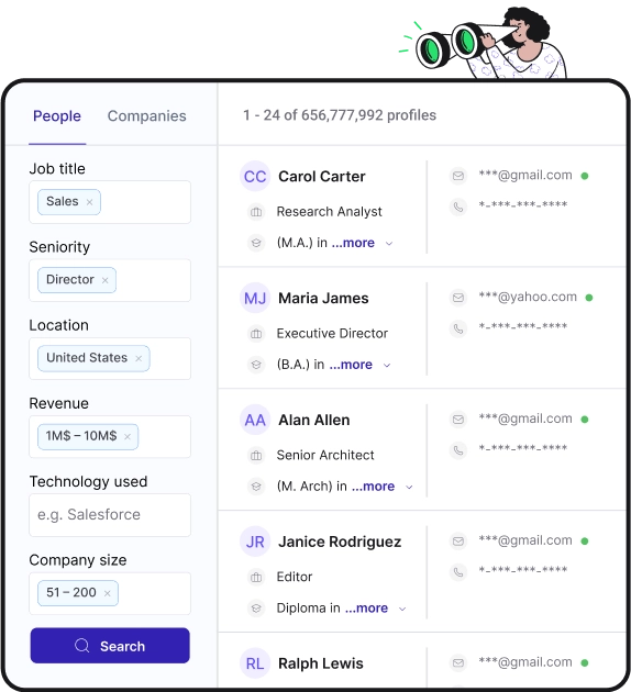
Scott Williams's Email Addresses
Find personal and work emails for over 300M professionals
Not the Scott Williams you were looking for? Continue your search below:About Scott Williams
📖 Summary
Scott Williams is a former American professional basketball player who made a name for himself during his time in the NBA. Born on March 21, 1968, in Hinsdale, Illinois, Williams grew up with a love for basketball and went on to play for the University of North Carolina Tar Heels under the legendary coach Dean Smith. Williams was a standout player at UNC, helping the Tar Heels win the NCAA Championship in 1991. His strong performances on the court caught the attention of NBA scouts, leading to his eventual entry into the professional basketball world.
In 1990, Williams entered the NBA draft and was selected by the Chicago Bulls in the second round. He joined a team that would soon become one of the most iconic in NBA history, led by the legendary Michael Jordan. Williams quickly made his mark as a valuable member of the Bulls, contributing to their success during the early 1990s. His athleticism, strong defensive skills, and ability to grab rebounds made him a key player off the bench for the Bulls, and he played a pivotal role in the team's three consecutive NBA Championships from 1991 to 1993.
After his successful stint with the Bulls, Williams went on to play for several other NBA teams, including the Phoenix Suns, the Dallas Mavericks, and the Milwaukee Bucks. Throughout his career, Williams was known for his tenacity on the court, giving his all in every game and earning the respect of teammates and opponents alike. His durability and work ethic made him a valuable asset to every team he played for, and his contributions did not go unnoticed by fans and coaches.
Williams' career highlights include winning three NBA Championships with the Bulls and making significant contributions to the success of each team he played for. He was known for his ability to come off the bench and make an immediate impact, bringing energy and intensity to the game. His solid defensive play and knack for grabbing key rebounds often shifted the momentum in his team's favor, making him a reliable and respected player throughout his time in the NBA.
After retiring from professional basketball, Williams pursued a career in broadcasting and coaching, sharing his knowledge and passion for the game with the next generation of players. He remained involved in the basketball community, using his experience and insight to mentor young athletes and help them develop their skills on and off the court. Williams' impact on the sport extended beyond his playing days, as he continued to inspire and influence others through his work in broadcasting and coaching.
Overall, Scott Williams' career as an American basketball player left an indelible mark on the NBA. His contributions to the success of multiple teams and his dedication to the sport have solidified his legacy as a respected and admired figure in basketball. With his unwavering determination and commitment to excellence, Williams exemplified the best qualities of a professional athlete and continues to be remembered as a true icon of the game.
Scott Williams's Email Addresses
People you may be
interested in
International airline
American actress
Singer and songwriter
Author
American basketball player
American actor and filmmaker
Indian actor and martial artist

President & CEO at SportsRantz.com

Father, Hall of Famer, six-time NBA champion, Olympic gold medalist, 50 greatest | UNGUARDED available now!

Entrepreneur with a big heart. TV * Media * V.O

Blogger

TRADER na BOVESPA